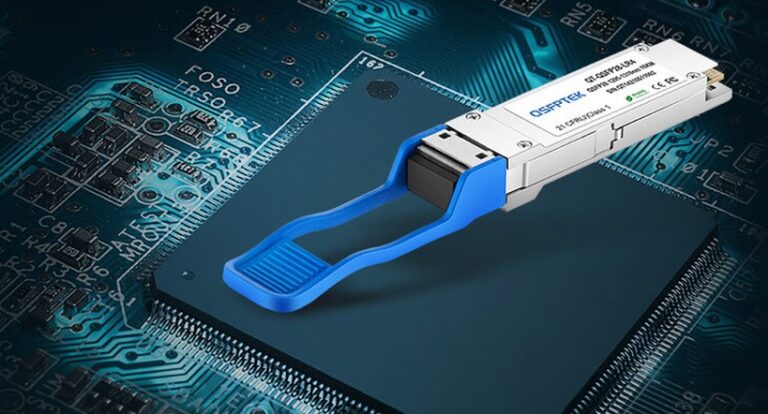
In recent years, the continuous progress of communication technology has brought about the vigorous development of big data applications. The demand for high-speed optical modules in communication base stations and data centers is becoming increasingly urgent.
Due to the technical level of the chip, for optical modules with 40G (click here) or higher speed, the speed of a single laser chip cannot meet the requirements of the overall communication rate. In order to solve this contradiction, the industry has developed a parallel multi-channel optical module, that is, multiple laser chips are integrated into one optical module, and the overall transmission rate requirements are met by multi-channel parallel transmission.
With the increasing number of parallel integrated channels in the optical module, a new problem arises – because more optical chips are integrated into the multi-channel optical module, the heat dissipation pressure in the module is much greater than that in the low-speed module. If good heat dissipation cannot be guaranteed, heat will accumulate in a large amount inside the module. The high temperature will lead to a series of performance deterioration, such as the rise of the threshold current of the laser chip, the decline of efficiency, and the drift of the detector chip responsiveness. In severe cases, the chip will fail, and the module performance and reliability will face great challenges.
The new integrated architecture of parallel multi-channel optical modules
To solve these problems, a new integrated structure of multi-channel optical modules with high heat dissipation and high integration is studied in this paper. This structure has an efficient internal heat export capability and does not occupy the wiring space between the interior and the surface of the PCB. More electrical signal pins are used to adapt to the integration of optical modules with more channels. The power device 300 is placed on the insulating high thermal conductivity block 800. The insulating high thermal conductivity block 800 uses high thermal conductivity ceramic materials – AlN ceramics, SiC ceramics, or BeO ceramics. The installation area of the power device 300 on the back of the insulating high thermal conductivity block 800 is processed with a metalized pad. The power device 300 and the insulating high thermal conductivity block 800 are fixed together by AuSn eutectic welding or high thermal conductivity Ag adhesive bonding.
The optical module housing 500 is processed into a ladder shape, and the PCB 200a is installed on the deeper cavity surface of the optical module housing 500. One part of the insulating high thermal conductivity block 800 is placed on the PCB 200, and the other part is placed on the shallow cavity surface of the optical module housing 500. The area where the front face of the insulating high thermal conductivity block 800 overlaps the optical module housing 500 is processed with a metallized pad. The surface of the optical module housing 500 is subject to weldable electroplating treatment (such as nickel plating). The insulating high thermal conductivity block 800 and the optical module housing 500 are brazed by adding SnPb solder. The insulating high thermal conductivity block 800 and PCB 200a are bonded and fixed with high-strength insulating glue.
On the back of PCB 200b, a dot matrix pad array 2001 is processed as the external electrical signal pin of the optical module. The optical module housing 100 needs to open a window at the corresponding position of the dot matrix pad array 2001 so that the dot matrix pad array 2001 can be exposed. The circuit connection between the power device 300 and the PCB 200a is realized by gold wire 300a bonding. The flexible interconnection between PCB 200a and PCB 200b is realized through flexible PCB 200c.
The optical elements used to realize the optical path interconnection between the optical chip (included in the power device) inside the optical module and the optical fiber can adapt the optical lens group 600 with an integrated multi-channel optical path or the multi-channel optical fiber array 900. If the optical lens group 600 is used, its mounting surface can be designed into a ladder shape according to the thickness of the insulating high thermal conductivity block 800. During installation, high-strength glue is used for bonding, and part of it is installed on the insulation high heat conduction block 800, and the other part is installed on the PCB 200a. If multi-channel optical fiber array 900 is used, the multi-channel optical fiber array 900 can be directly installed on the insulating high thermal conductivity block 800, which can be bonded or welded with high-strength glue.
Application examples and test results
In this paper, a parallel 24-channel optical transceiver product is designed with the above new integrated structure of a multi-channel optical module with high heat dissipation capability and high integration. The module adopts the internal structure design shown in Figure 2, the optical path coupling part adopts the integrated multi-channel lens group, and the electrical signal output structure adopts the 200pin metal reed connector. Module size is less than 25 mm × 21 mm × 8 mm, the number rate of a single channel is 10.315 Gbps, and the total power consumption of the module is 2.4 W.
Because the insulating high thermal conductivity block is used as the main heat dissipation medium, the heat generated by the power device can be directly transmitted to the optical module shell through the insulating high thermal conductivity block. The insulating high thermal conductivity block has the characteristics of high thermal conductivity, with the highest thermal conductivity of more than 270 W/m • K (170-200 W/m • K for AlN ceramics, 270 W/m • K for BeO ceramics, and 83 W/m • K for SiC ceramics), which is far superior to the heat dissipation capacity of the dense copper vias in the PCB in the traditional COB scheme, and can efficiently derive the heat generated by the power devices inside the optical module. As the heat dissipation capacity of the optical module is greatly improved, it is particularly suitable for integrating high-speed optical modules with more channels. Better heat dissipation capability can reduce the working temperature of the chips inside the optical module (especially the laser chip), thus extending the service life of the optical module, and can expand the use temperature range of the optical module.
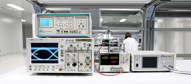
The module is tested for heat dissipation pressure in a high-temperature environment. When the module shell temperature is 70 ℃, the loop-back test results are shown in Figure 6. It can be seen from the test results that for the PRBS 31 code type, the speed of the module at high temperature is 10.312 5 Gbps, and the sensitivity is better than – 11 dBm when the error rate of the loopback test is better than 10-12. It indicates that the heat dissipation capacity of the module is good, and the performance index has not deteriorated under the high-temperature working condition of 70 ℃ shell temperature.